
Understanding Microcontroller Architecture: A Complete Guide
What is Microcontroller Architecture?
Defining the “Computer on a Chip”
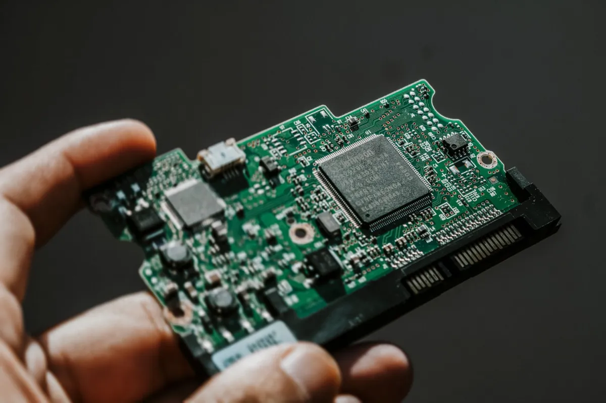
At its core, a microcontroller (MCU) is a single silicon die that contains a processor, memory, and a suite of peripherals. It can fetch instructions from non‑volatile storage, execute them, and interact with the physical world through I/O pins—all without needing an external chipset.
A microcontroller architecture describes how these blocks are organized, connected, and accessed by software. It defines the instruction set, bus structure, memory map, and the set of built‑in hardware modules that a programmer can control.
The Difference Between Microprocessors and Microcontrollers
A microprocessor (MPU) supplies only the CPU. Designers must add external RAM, Flash, and peripheral chips on a motherboard. In contrast, a microcontroller integrates all those pieces on the same die, resulting in lower cost, smaller board size, and deterministic real‑time behavior.
Why Architecture Matters in Modern Embedded Systems
Choosing the right architecture influences power consumption, code density, development tooling, and the ability to meet timing constraints. An MCU with a well‑designed clock tree and DMA engine can run a sensor hub at a fraction of the energy budget of a less efficient design.
Core Components of a Microcontroller
The Central Processing Unit (CPU): The Brain
The CPU core fetches, decodes, and executes instructions. Modern MCUs use ARM Cortex‑M series cores (M0+, M3, M4, M7, and the newest M55 with Helium vector extensions), RISC‑V cores (e.g., SiFive E21/E31), or proprietary 8‑bit cores such as Microchip’s PIC16. The core defines the register set, pipeline depth, and optional hardware accelerators (FPU, DSP, crypto).
Memory Organization: Flash, RAM, and EEPROM
Flash stores program code and constant data. SRAM holds the stack, heap, and runtime variables. Some MCUs add EEPROM or FRAM for byte‑addressable non‑volatile storage. Memory is typically mapped into a flat address space, but many 8‑bit devices keep program memory separate (Harvard style).
Input/Output (I/O) Ports and GPIOs
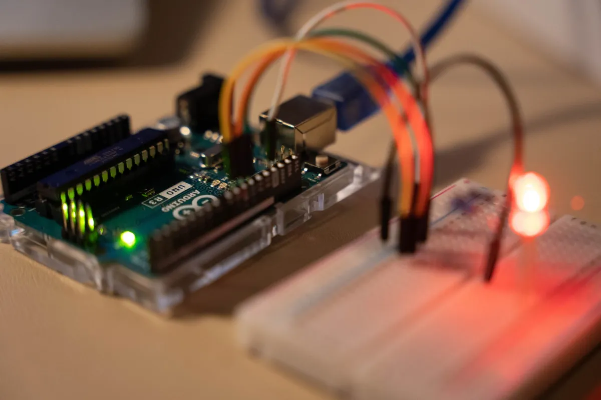
General‑purpose I/O pins are multiplexed with peripheral functions (UART, SPI, CAN, etc.) through alternate‑function registers. Each pin can be configured for pull‑up/down, drive strength, and interrupt edge detection.
Timers, Counters, and Interrupt Controllers
Timers generate precise time bases, PWM signals, and capture events. The interrupt controller—NVIC on Cortex‑M or PIC’s INTCON—prioritizes and dispatches interrupt requests. Advanced MCUs support nested, preemptive interrupts and priority grouping, allowing a high‑frequency peripheral (e.g., UART) to pre‑empt a lower‑priority task (e.g., ADC conversion complete).
Analog-to-Digital Converters (ADC) and DACs
Integrated ADCs convert analog sensor voltages to digital words, often with selectable resolution (8–16 bits) and sampling rates up to several megasamples per second. DACs provide analog output for control loops or audio generation.
Clock System and Power Management
The clock tree distributes timing sources to the CPU and peripherals. Typical sources include an internal RC oscillator, an external crystal (e.g., 8 MHz), and a PLL that multiplies the base frequency. Each peripheral can be fed from a dedicated prescaler, enabling fine‑grained power control. Low‑power domains (e.g., a 32.768 kHz RTC oscillator) stay active while the core sleeps.
Bus Matrix and DMA Engine
A high‑performance bus matrix arbitrates access between masters (CPU, DMA, DMA‑capable peripherals) and shared memory. DMA channels move data between memory and peripherals without CPU intervention, drastically reducing latency and power consumption for high‑throughput tasks such as audio streaming or sensor data acquisition.
Comparing Major Architectural Paradigms
Von Neumann vs. Harvard Architecture
In a Von Neumann layout, program and data share a single bus and memory space. This simplicity can cause a bottleneck when the CPU tries to fetch an instruction and read/write data simultaneously. Harvard architecture separates instruction and data paths, allowing parallel access and higher throughput.
| Aspect | Von Neumann | Harvard |
|---|---|---|
| Bus Structure | Single shared bus | Separate instruction & data buses |
| Memory Space | Unified address space | Distinct address spaces (or tightly‑coupled memory) |
| Typical Use | General‑purpose CPUs, some low‑cost MCUs | Modern 32‑bit MCUs, DSPs, high‑speed peripherals |
| Performance Impact | Potential “Von Neumann bottleneck” | Simultaneous fetch and data access |
RISC vs. CISC: Efficiency and Instruction Sets
RISC cores use a small, uniform instruction set that executes in one or two cycles, simplifying pipelines and enabling low power. CISC cores pack more work into each instruction, which can reduce code size but often require more complex decoding logic.
| Feature | RISC | CISC |
|---|---|---|
| Instruction Length | Fixed (usually 16‑ or 32‑bit) | Variable (1–15 bytes) |
| Typical Cycle Count | 1–2 cycles per instruction | Multiple cycles, variable decode |
| Code Density | Lower, more instructions needed | Higher, complex instructions compress code |
| Power Consumption | Generally lower | Higher due to complex decode |
| Examples (2026) | ARM Cortex‑M0+, RISC‑V E21/E31 | Intel 8051‑compatible cores, some legacy PIC24 |
CISC: Complex Instruction Set Computing
Although most new MCUs favor RISC cores, a few families retain CISC‑style instruction sets for backward compatibility. These devices often include rich addressing modes and built‑in multiply‑accumulate instructions that simplify certain algorithms at the cost of higher silicon area.
RISC: Reduced Instruction Set Computing
RISC dominates the MCU market in 2026. ARM’s Cortex‑M series offers deterministic latency, optional hardware divide, and optional floating‑point units. RISC‑V provides an open ISA, modular extensions (e.g., “P” for packed SIMD), and a growing ecosystem of open‑source cores.
Modern Trends in 2026 Microcontroller Design

The Rise of ARM Cortex‑M and RISC‑V
ARM Cortex‑M remains the workhorse for 32‑bit MCUs, with the Cortex‑M55 introducing matrix‑multiply extensions for TinyML. RISC‑V has entered mainstream production; vendors such as SiFive, GigaDevice, and Western Digital now ship 64‑KB to 2‑MB flash parts with integrated peripherals.
Integration of AI Accelerators and TinyML
Edge AI demands inference at micro‑watt levels. New MCUs embed neural‑network accelerators (e.g., ARM’s Ethos‑U55, RISC‑V’s “Ve” vector extension) that can execute 8‑bit quantized models in under 1 ms. These accelerators share the same bus matrix, and developers can offload convolution layers via DMA.
Ultra‑Low Power Architecture for IoT Edge Devices
Power‑gated domains, sub‑microwatt sleep modes, and adaptive voltage scaling have become standard. Devices like the STM32L5 and the ESP32‑C3 can run for years on a coin cell while still supporting BLE 5.3.
Multi‑core MCU Architectures
Dual‑core designs (e.g., Cortex‑M7 + Cortex‑M0+ in the same die) allow a high‑performance core to handle signal processing while the low‑power core manages sensor acquisition and sleep‑state orchestration. The cores communicate via a shared memory region and a hardware semaphore.
Best Practices for Choosing the Right Architecture
Matching Memory Requirements to Application Needs
- Calculate the total size of your code (.text) and constant data (.rodata). Add a 20 % safety margin for future updates.
- Estimate RAM usage: stack, heap, and any large buffers (e.g., audio samples). Use the linker map file to verify.
- Select an MCU with flash and SRAM that exceed these estimates. Consider external SPI‑Flash if on‑chip memory is insufficient.
Evaluating Power Consumption vs. Performance
Use the vendor’s power calculator to compare active, sleep, and deep‑sleep currents. Remember that enabling a peripheral’s clock keeps it alive; disable unused clocks via the RCC (Reset & Clock Control) registers.
Considering Peripheral Availability
Check the peripheral matrix for required interfaces (UART, SPI, I²C, CAN, USB, Ethernet, etc.). Verify that the pins you need are not locked in an alternate function that conflicts with your design.
Software Ecosystem and Toolchain Support
A robust HAL, middleware (FreeRTOS, CMSIS‑DSP), and IDE (STM32CubeIDE, VS Code with PlatformIO) reduce time‑to‑market. Open‑source RISC‑V tools (GNU Toolchain, Zephyr) have matured, making the ecosystem comparable to ARM.
Common Pitfalls and Troubleshooting
Memory Overflow and Stack Overruns
Large local arrays or deep recursion can exceed the limited SRAM stack. Enable stack canaries in your compiler settings and monitor the stack pointer during debugging.
Interrupt Latency and Priority Conflicts
On Cortex‑M devices, the NVIC allows priority grouping. A common mistake is configuring two high‑frequency sources (e.g., UART Rx and TIM update) at the same priority, causing missed events. Use NVIC_SetPriority() to assign distinct levels.
Clock Configuration Errors
Failing to enable the peripheral clock before accessing its registers results in “dead” peripherals. The following snippet shows the correct sequence for an STM32L4 UART:
#include "stm32l4xx.h"

void uart_init(void) {
 /* 1. Enable GPIOA clock */
 RCC->AHB2ENR |= RCC_AHB2ENR_GPIOAEN;

 /* 2. Enable USART2 clock */
 RCC->APB1ENR1 |= RCC_APB1ENR1_USART2EN;

 /* 3. Configure PA2 (TX) and PA3 (RX) alternate function */
 GPIOA->AFR[0] |= (7 << (2 * 4)) | (7 << (3 * 4)); // AF7 = USART2
 GPIOA->MODER |= (2 << (2 * 2)) | (2 << (3 * 2)); // Alternate mode

 /* 4. Set baud rate (e.g., 115200) assuming 80 MHz PCLK1 */
 USART2->BRR = 80e6 / 115200;

 /* 5. Enable USART, TX and RX */
 USART2->CR1 = USART_CR1_TE | USART_CR1_RE | USART_CR1_UE;
}
Power Leakage in Sleep Modes
Even in deep‑sleep, stray currents can flow through improperly configured pins (e.g., floating analog inputs). Set unused GPIOs to analog mode or enable pull‑downs before entering Stop mode.